Development of Micro- and Nano-fabrication Technologies: including controlled nano-fabrication, inkjet micro-fabrication, 3D fabrication by micro-electro-discharge machining, catalytic chemical vapor deposition of carbon nanotubes, Si nanowire growth, high resolution lithography and microscopy, microfluidic devices.
Faculty Involved
Research Topics
Carbon Nanotubes
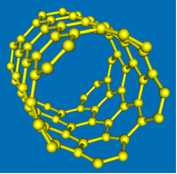
Carbon nanotubes, nanometer-diameter tubes made of carbon atoms, have been gaining ever-increasing popularity since their discovery in 1991 due to their outstanding electronic and mechanical properties. Nanotubes can be used in a wide range of applications including electronic devices such as quantum dots and transistors, electron emitters for flat-panel displays and electron-beam systems, chemical and biological sensors, light-weight composites and nanoscale actuators to name a few.
Electron Sources
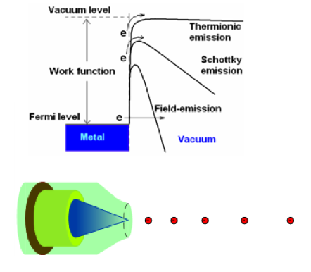
Electrons can be emitted from a material into vacuum by heating the material to very high temperatures (thermionic emission), the application of a strong external field (field-electron emission), illumination by light (photo-electron emission), or a combination of these. Electron sources are in high demand in applications such as vacuum tubes, electron microscopy and lithography equipment for micro/nanofabrication, field-emission displays, synchrotrons, electron holography and interferometry, and vacuum nano-electronics.
Flexible Electronics
Inkjet Technology
Inkjet technology printing provides a very versatile and low-cost microfabrication capability that has attracted significant research and industrial interest. Inkjet technology can be used to pattern a variety of liquids including polymers, proteins, and various solvents. This technique is used for non-contact patterning onto rigid, flexible, rough, smooth, and 3-D substrates. This process is accurate, high resolution, high speed, and consumes very little material as compared to a lithographic process. As a result, inkjet fabrication can be used for rapid prototyping and is capable of producing large batches of device variants that can later be grouped and evaluated based on various performance characteristics. The inks can be fused with nanostructures such as nanowires, nanotubes, and quantum dots to modify material properties targeting new applications. Inkjet technology has already been widely applied to the fabrication of polymer transistors, organic light emitting diodes (OLEDs), artificial tissue scaffolds, polymer sensors, and many other devices. MiNa members are using this technology to fabricated polymer based devices such as transistors, and chemical sensors. As well, we are using this technology to explore novel frontiers of biology such as constructing tissue scaffolds and printing cells.
Micro Electro-discharge Machining
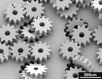
Micro electro-discharge machining (micro-EDM) utilizes high-frequency pulses of ultimately miniaturized spark discharge to thermally remove the target material using microscopic electrodes. Micro-EDM is a very powerful technique for micro-scale engineering because it can be used to micromachine any type of electrical conductors. This capability can potentially be exploited to vastly expand the material base of MEMS, offering a variety of new application opportunities for MEMS. The research is pushing the limit toward high throughput and nano domain and exploring the application with a focus on biomedical devices such as sensor-integrated antenna stents.
Nanowires
Organic Materials
Research Projects
Protein-based Solar Cell
Plants capture photons very efficiently. Can we learn from them in making photovoltaic devices? We are investigating the use of photosynthetic protein complexes in solar cells, with the aim of creating very low cost solar cells.