Education
Research Areas
Group Members
Alumni
Bio
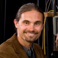
Lukas Chrostowski is a Professor of Electrical and Computer Engineering at the University of British Columbia, Vancouver, BC, Canada. Born in Poland, he earned the B.Eng. in electrical engineering from McGill University and the PhD in electrical engineering and computer science from the University of California at Berkeley. With research interests in silicon photonics, optoelectronics, high-speed laser (VCSEL) design, fabrication and test, for applications in optical communication systems and biophotonics, he has published more than 200 journal and conference publications. He co-edited a book “High-Speed Photonics Interconnects” (2013), and co-authored the book “Silicon Photonics Design” (Cambridge University Press, 2015). Dr. Chrostowski served as the co-director of the University of British Columbia AMPEL Nanofabrication Facility (2008-2017). He is the Program Director the NSERC CREATE Silicon Electronic-Photonic Integrated Circuits (Si-EPIC) research training program in Canada, and has been teaching numerous silicon photonics workshops and courses since 2008. He spent his 2011-12 sabbatical at the University of Washington, Seattle, with Michael Hochberg’s group. Chrostowski received the Killam Teaching Prize at the University of British Columbia in 2014. He was an elected member of the IEEE Photonics 2014-2016 Society Board of Governors and serves as the Associate VP of Education (2014-). He was awarded a Natural Sciences and Engineering Research Council of Canada Discovery Accelerator Supplements Award in 2015.
Research Interests
My primary research area is in silicon photonics. Read more about it in my textbook – Silicon Photonics Design by Cambridge Press. The applications of this technology that I am interested in are: 1) communications, including short reach data communications, long distance communications, and microwave photonics; 2) biosensors, 3) quantum information.
At UBC, we have facilities to design, fabricate, and test silicon photonic devices and circuits.
Quantum silicon photonics: Using the relatively mature silicon photonics technology, and very mature CMOS electronics technology, we are aiming to implement a quantum computer. We are using a cavity quantum electrodynamics (cQED) approach with single atoms implanted in silicon as qubits, 4K cryogenic operation in vacuum, mid-IR wavelengths, single photon sources and detectors, and possibly NEMS. We are quickly assembling a world-class team to tackle this immense challenge.
We need intense efforts in developing process design kits and Libraries using detailed electromagnetic device design, together with achieving significant process improvements in electron beam lithography fabrication necessary to realize the quantum silicon photonics vision.
We are recruiting in the areas of:
- photonic device design
- photonic circuit design
- computational electromagnetics
- fabrication process innovation, statistical process control
- experimental equipment design and development, including automation, cryogenics, laser design
- photonic characterization and control
- packaging and integration with external optics and electronics
Courses
Projects
Publications
For an updated list of citations, visit my profile on Google Scholar.